The 700°C Chip: A Breakthrough in Extreme-Temperature Electronics
Engineers have shattered a fundamental barrier in electronics by creating a memory device that operates reliably at 700°C (1300°F), a temperature hotter than molten lava. This breakthrough, achieved through an innovative material stack of tungsten, hafnium oxide, and graphene, prevents atomic-level heat failure and opens new frontiers for computing in extreme environments. The technology promises to transform space exploration, geothermal energy, and AI processing by enabling electronics to function where traditional silicon chips cannot survive.
For decades, the relentless enemy of all electronics has been heat. Once temperatures climb beyond roughly 200°C, the delicate structures within silicon chips begin to degrade, leading to catastrophic failure. This thermal barrier has constrained innovation in fields from deep-space exploration to advanced industrial systems. Now, a team of engineers has achieved what was once thought impossible: a functional memory device that not only survives but thrives at a staggering 700°C (1300°F). This breakthrough, detailed in a 2026 study published in Science, represents a quantum leap in material science and electronic engineering, potentially redefining the operational limits of future technology.
The Anatomy of a Heat-Proof Memory Device
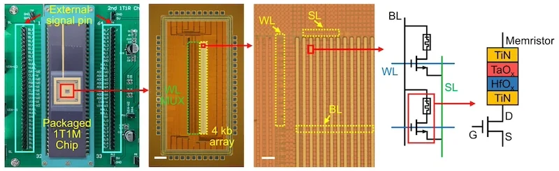
The revolutionary component is a type of memristor, a nanoscale device capable of both data storage and computation. Its resilience stems from an unconventional material architecture. The top electrode is constructed from tungsten, the element with the highest known melting point. Sandwiched in the middle is a thin ceramic layer of hafnium oxide. The foundational layer, however, is the key: a single-atom-thick sheet of graphene. This combination was not the initial target of the research but emerged from an accidental discovery during experiments at the University of Southern California.
As lead researcher Professor Joshua Yang noted, the finding was serendipitous, a common trait of significant scientific leaps. The device demonstrated exceptional performance, retaining data for over 50 hours at the peak test temperature of 700°C without requiring a refresh. It also endured more than one billion operational cycles at this extreme heat, all while operating at a low voltage of 1.5 volts and achieving speeds in the tens of nanoseconds.
The Atomic Mechanism Behind the Heat Resistance
The true innovation lies in the atomic interaction at the material interfaces. In standard electronics, intense heat causes metal atoms from the top electrode to migrate through the middle layer. Eventually, they reach the bottom electrode, forming a permanent conductive bridge that shorts the circuit, leaving the device stuck in an "on" state. The graphene layer in this new design completely prevents this failure mode.
.jpg)
Professor Yang describes the interaction between tungsten and graphene as similar to oil and water. Tungsten atoms that drift toward the graphene surface cannot find a stable attachment point. Without a foothold, they simply drift away, unable to form the destructive short-circuit bridge. This interfacial engineering, confirmed through advanced electron microscopy and quantum simulations, is the fundamental principle that grants the device its unprecedented thermal stability. This understanding provides a blueprint for identifying other material pairs with similar repulsive properties, paving the way for scalable manufacturing.
Transformative Applications in Extreme Environments
The implications of electronics that can operate above 500°C are profound and wide-ranging. The most immediate application is in space exploration. The surface of Venus, for instance, maintains temperatures around 465°C, and every lander sent to the planet has succumbed to the extreme heat. This new technology could enable long-duration missions and surface operations on Venus and other high-temperature planetary bodies.
On Earth, the benefits are equally significant. Geothermal energy systems, which tap into the intense heat deep within the planet, require monitoring and control electronics that can function in red-hot boreholes. Similarly, next-generation nuclear and fusion reactors expose equipment to extreme thermal conditions. Even in more conventional settings, such as under the hood of a modern vehicle where temperatures can reach 125°C, a device rated for 700°C would offer exceptional longevity and reliability, virtually eliminating heat-related failures.
Accelerating Artificial Intelligence with Efficient Computing
Beyond mere survival, this memristor technology offers a paradigm shift for artificial intelligence processing. A significant portion of AI computation, over 92% in systems like ChatGPT according to the research, involves matrix multiplication. Traditional von Neumann architectures perform these calculations sequentially, shuttling data between separate memory and processing units—a process that consumes substantial time and energy.

Memristors operate on a principle of in-memory computing. By leveraging Ohm's Law (current = voltage × conductance), they can perform matrix multiplication directly as electrical current flows through the device network. The result is obtained almost instantaneously as a measured current, bypassing the data transfer bottleneck. This approach promises orders-of-magnitude improvements in speed and energy efficiency for AI tasks. Professor Yang and colleagues have already co-founded a company, TetraMem, to commercialize room-temperature memristor AI chips. The high-temperature variant could allow for advanced, on-site AI processing in the very extreme environments where it is needed most, such as on autonomous spacecraft or deep-earth sensors.
The Path from Laboratory Prototype to Widespread Adoption
While the results are groundbreaking, researchers caution that practical, integrated systems are still on the horizon. A functional memory device is only one component of a complete computer. High-temperature logic circuits, processors, and supporting architecture must still be developed and seamlessly integrated with this memory technology. Furthermore, the current devices were fabricated manually at a small scale in a lab. Transitioning to cost-effective, high-volume semiconductor manufacturing will be a significant engineering challenge.
However, the path is clearer than ever. Two of the core materials, tungsten and hafnium oxide, are already staples in existing semiconductor fabrication lines. Graphene, while newer, is under active development by industry giants like TSMC and Samsung and has been produced at the wafer scale in research settings. The foundational barrier—a reliable high-temperature memory—has been removed. As Professor Yang stated, this is the critical first step that makes everything else logically possible.
This research, conducted through the CONCRETE Center with support from the Air Force Office of Scientific Research, marks the beginning of a new frontier in electronics. It moves the goalposts from managing heat to outright conquering it, enabling a future where advanced computing can accompany humanity into the most inhospitable and energy-intensive corners of the universe and our own planet. The 700°C chip is not just a component; it is a key that unlocks a world of previously impossible technological endeavors.