3D Nanolithography Breakthrough: Metalens Arrays Enable Wafer-Scale Fabrication
A revolutionary 3D nanolithography platform using metalens arrays and adaptive illumination has achieved unprecedented throughput and precision, enabling wafer-scale production of complex nanostructures. This breakthrough technology overcomes fundamental limitations of conventional methods by generating over 120,000 cooperative focal spots simultaneously, achieving throughput exceeding 100 million voxels per second. The system demonstrates centimeter-scale 3D architectures with feature sizes down to 113 nanometers, opening new possibilities for microelectronics, biomedicine, quantum technology, and advanced materials manufacturing.
The field of nanofabrication has reached a pivotal moment with the development of a revolutionary 3D printing platform that promises to transform how we manufacture complex micro- and nanostructures. Traditional 3D laser nanofabrication techniques, particularly two-photon lithography (TPL), have long faced fundamental challenges in scaling due to field-of-view limitations of conventional imaging optics. These limitations result in throughput constraints, proximity errors, and stitching defects that have prevented wafer-scale production of intricate 3D architectures. Now, researchers have developed a scalable solution that combines metalens-generated focal spot arrays with spatially adaptive illumination to overcome these barriers.

The Metalens Advantage in Nanolithography
Metalenses represent a paradigm shift in optical engineering, offering unique advantages that make them ideally suited for high-throughput nanolithography. Unlike conventional refractive lenses, metalenses use nanostructured surfaces to manipulate light with subwavelength precision. This technology enables large numerical apertures (NAs), compatibility with immersion media, and most importantly, large-scale manufacturability. The breakthrough system described in Nature utilizes a 12-cm² metalens array to produce more than 120,000 cooperative focal spots simultaneously. This massive parallelization represents a quantum leap in fabrication capability, achieving throughput exceeding 10⁸ voxels per second.
Adaptive Parallel Printing Strategy
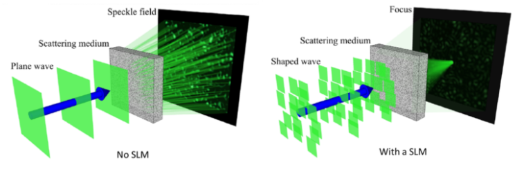
The true innovation of this platform lies in its adaptive parallel printing strategy. By programmatically patterning the focal spot array using a spatial light modulator (SLM), researchers can achieve precise greyscale linewidth modulation and choreographed printing of both semiperiodic and fully aperiodic 3D geometries. This adaptive approach allows for dynamic control over individual focal spots, enabling the fabrication of structures with varying densities and complex spatial arrangements without the stitching defects that plague conventional methods.
Demonstrated Capabilities and Applications
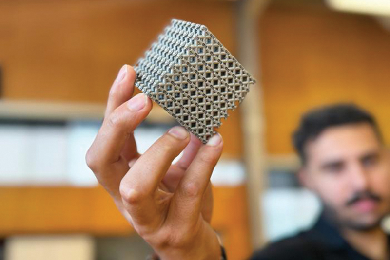
The experimental demonstrations of this technology showcase its transformative potential. Researchers have successfully printed replicated microstructures at rates exceeding 50 million microparticles per day, centimeter-scale 3D architectures with feature sizes down to 113 nanometers, and sophisticated photonic and mechanical metamaterials. These achievements represent orders of magnitude improvement over existing TPL systems and open new avenues for applications across multiple fields.
Microelectronics and Quantum Technology
For microelectronics, this technology enables the fabrication of complex 3D interconnects, advanced packaging architectures, and novel device structures that were previously impossible to manufacture at scale. In quantum technology, the precision and scalability offered by metalens-based TPL could accelerate the development of quantum information systems, including 3D-printed micro ion traps and other quantum device components.
Biomedicine and Advanced Materials
In biomedicine, the ability to create intricate 3D structures at the nanoscale opens possibilities for tissue engineering scaffolds, drug delivery systems, and medical implants with precisely controlled mechanical and biological properties. The technology also enables the production of mechanical metamaterials with tailored properties for applications ranging from energy absorption to flexible electronics.
Technical Implementation and System Architecture
The metalens-based TPL system integrates several advanced optical components to achieve its remarkable performance. A key element is the phase-to-amplitude modulation subsystem that uses liquid-crystal SLMs to precisely control laser intensity. This subsystem, combined with carefully designed 4f optical systems, enables the generation of complex intensity patterns across the metalens array. The metalenses themselves are fabricated using advanced nanolithography techniques, with designs optimized for specific numerical apertures and immersion conditions.
Future Prospects and Scaling Potential
The current implementation represents just the beginning of what's possible with metalens-based nanolithography. Researchers project that further optimization and scaling could push throughput even higher, potentially enabling true wafer-scale production of 3D nanostructures. The technology's compatibility with existing semiconductor manufacturing processes suggests a relatively straightforward path to industrial adoption. As metalens fabrication techniques continue to improve and costs decrease, this platform could become a standard tool for advanced manufacturing across multiple industries.
Conclusion
The development of 3D nanolithography with metalens arrays and spatially adaptive illumination marks a watershed moment in nanofabrication technology. By overcoming the fundamental throughput and scaling limitations of conventional methods, this platform enables the production of complex 3D architectures at scales and speeds previously unimaginable. As research continues and the technology matures, we can expect to see transformative applications in microelectronics, biomedicine, quantum technology, and materials science. This breakthrough not only advances the state of the art in nanofabrication but also opens new frontiers in what's possible to design and manufacture at the nanoscale.