The 3D Chip Revolution: Breaking AI's Memory Bottleneck
A breakthrough in semiconductor design from a U.S. research consortium has produced a monolithic 3D computer chip that vertically stacks memory and computing elements. This architecture, manufactured in a domestic foundry, dramatically accelerates data movement, overcoming the critical 'memory wall' that limits current AI hardware. Early prototypes show performance improvements of 4x over traditional 2D chips, with simulations projecting up to 12x gains. This innovation marks a pivotal shift towards domestic, high-performance AI hardware production.
The relentless advancement of artificial intelligence is hitting a fundamental hardware barrier: the physical design of the chips themselves. As AI models like ChatGPT demand ever-faster data processing, traditional flat, two-dimensional semiconductor architectures are struggling to keep pace, creating a critical bottleneck known as the "memory wall." However, a landmark development from a collaboration between Stanford University, Carnegie Mellon University, the University of Pennsylvania, MIT, and SkyWater Technology promises to shatter this barrier. They have successfully created and manufactured a new kind of monolithic 3D computer chip in a U.S. foundry, stacking memory and logic vertically to achieve order-of-magnitude performance gains and charting a new course for domestic semiconductor innovation.

The Fundamental Problem: The Memory and Miniaturization Walls
Modern AI's hunger for data is insatiable. Large language models constantly shuttle enormous volumes of information between memory storage and the computing units that process it. On conventional 2D chips, all these components sit on a single plane. Memory is limited and physically spread out, forcing data to travel through a small number of long, congested pathways. This creates a severe mismatch: the computing processors can operate far faster than data can be delivered to them, leading to frequent idle periods waiting for information. This bottleneck is the infamous "memory wall."
For decades, the industry's primary response was to shrink transistors and pack more onto each chip, a strategy now colliding with the "miniaturization wall"—hard physical limits that make further shrinkage increasingly difficult and costly. As researchers note, this combination forms a "deadly" constraint on progress. The new 3D design directly attacks both limitations by abandoning the flat paradigm and building upward, integrating memory and computation in a tightly woven, vertical structure.

Architectural Innovation: Building the Manhattan of Computing
The prototype chip represents a shift from 2D to 3D integration. Ultra-thin layers of circuitry are stacked like floors in a skyscraper, with dense vertical wiring acting as high-speed elevators that move massive amounts of data between layers. This approach places memory cells directly above or below the computing units that need them, drastically shortening the distance data must travel.
A key differentiator is the "monolithic" manufacturing process. Instead of creating separate chips and bonding them together—a method that often results in coarse, bottleneck-prone connections—this team builds each new layer directly atop the previous one in a single, continuous fabrication flow. This monolithic 3D integration uses low-temperature processes that don't damage the circuitry below, enabling extremely dense packing and a record number of vertical interconnects. As Professor Tathagata Srimani of Carnegie Mellon University explains, the design allows movement of "a lot more information much quicker, just as the elevator banks in a high-rise let many residents travel between floors at once."
Domestic Manufacturing and Performance Results
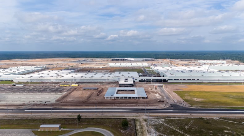
Perhaps as significant as the architectural breakthrough is where it was made. The entire chip was fabricated at SkyWater Technology's Bloomington, Minnesota foundry, the largest exclusively U.S.-based pure-play semiconductor foundry. This demonstrates that such advanced architectures are not confined to academic labs but are ready for real-world, domestic production. Mark Nelson of SkyWater emphasized that turning a cutting-edge concept into a commercially viable product is a major challenge, and this success is crucial for keeping the U.S. at the forefront of semiconductor innovation.
In hardware tests, the prototype has already demonstrated a roughly fourfold performance improvement over comparable 2D chips. Simulations are even more promising, suggesting that as more layers are added, the design could achieve up to a twelvefold improvement on real AI workloads, including those derived from models like Meta's LLaMA. The researchers highlight a longer-term potential for 100 to 1,000-fold improvements in energy delay product (EDP), a key metric combining speed and energy efficiency.

Implications for the Future of AI Hardware
This development is more than an incremental step; it is a blueprint for a new era of chip design. By proving monolithic 3D integration is manufacturable, it provides a scalable path to meet the exponentially growing computational demands of future AI systems. As Subhasish Mitra of Stanford University states, "Breakthroughs like this are how we get to the 1,000-fold hardware performance improvements future AI systems will demand."
The shift also has strategic importance for U.S. technological sovereignty. It creates a viable pathway for designing and producing the world's most advanced chips on domestic soil, reducing reliance on foreign supply chains. Furthermore, it necessitates and is already spurring a new generation of engineers trained in 3D design and fabrication methods, supported by initiatives like the Microelectronics Commons AI Hardware Hub.
In conclusion, the successful creation of this monolithic 3D chip represents a pivotal moment. It offers a tangible solution to the most pressing hardware limitation in AI, delivers immediate performance gains with a roadmap for massive future improvements, and strengthens the foundation for a resilient, innovative U.S. semiconductor industry. The future of computing is not just smaller—it's taller.