Intel's Strategic Bet: New Arizona Fab and 18A Chips Aim to Revive American Chipmaker
Intel is making a critical strategic move with the operational launch of its Fab 52 semiconductor plant in Chandler, Arizona, marking a pivotal moment for the struggling American chipmaker. The facility represents Intel's bet on its new 18A process technology and innovative chip designs to compete in the rapidly evolving semiconductor landscape. This development comes amid significant government investment and industry scrutiny as Intel attempts to regain its competitive edge against global rivals like TSMC and capitalize on the AI-driven chip demand that has propelled competitors like Nvidia to unprecedented valuations.
Intel's Fab 52 semiconductor plant in Chandler, Arizona has officially begun producing its first chips, representing a crucial turning point for the American chipmaker as it seeks to reverse years of competitive challenges. The facility's operational status comes at a critical juncture for Intel, which has faced significant market pressure from competitors and recently received substantial government support through an unconventional bailout arrangement.

The Manufacturing Challenge
Intel's Fab 52 represents the company's most advanced chip manufacturing capability to date, utilizing the new 18A process technology that promises significant performance improvements. The facility spans approximately one million square feet as part of a larger complex that includes Fab 42 and the still-under-construction Fab 62. The manufacturing environment requires extreme precision and contamination control, with air being recycled every six seconds and all personnel required to wear specialized anti-contamination suits.
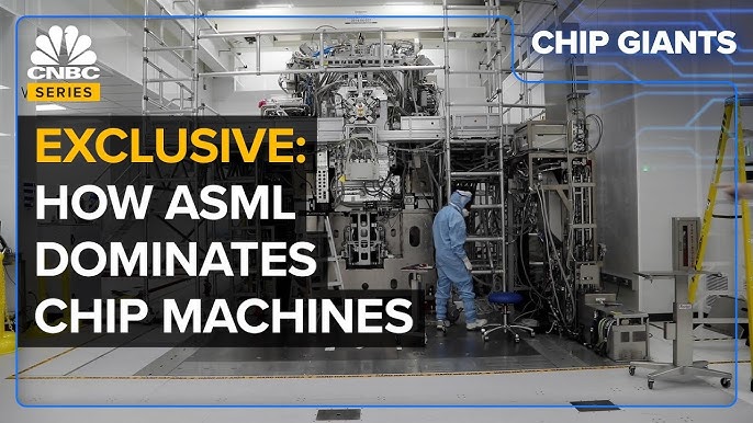
The semiconductor manufacturing process involves sophisticated robotic systems and massive lithography machines from suppliers like Dutch manufacturer ASML. These machines, some the size of school buses, print microscopic patterns on silicon wafers that form the foundation of modern computing. The entire operation depends on maintaining vibration-free environments and preventing even the smallest particle contamination that could ruin entire batches of chips.
Strategic Importance and Market Position
Intel's timing for showcasing Fab 52 reflects the company's urgent need to demonstrate its manufacturing capabilities amid intense competition. The facility's launch follows the Trump administration's acquisition of a 9.9 percent stake in Intel through an $8.9 billion stock exchange, representing a significant government vote of confidence in the American chipmaker. Additionally, Nvidia made a $5 billion strategic investment in Intel, signaling industry recognition of Intel's potential importance despite its recent struggles.
The company faces substantial market challenges, with its market capitalization falling below $100 billion while competitor Nvidia reached approximately $4 trillion valuation. Intel's difficulties trace back to missing the mobile computing revolution in the mid-2000s and subsequent failure to capitalize on emerging technology trends. The recent generative AI boom has further highlighted Intel's competitive disadvantages compared to companies like Nvidia and AMD that have captured the high-performance computing chip market.
Technological Innovation and Future Prospects
Intel's new Panther Lake and Clearwater Forest chips represent the company's technological response to market demands. These chips utilize Intel's innovative RibbonFET and PowerVia technologies, which fundamentally redesign transistor architecture and power delivery systems. RibbonFET stacks transistors for increased density, while PowerVia moves power interconnects to below the silicon stacks, potentially offering 30 percent energy efficiency improvements over previous generations.
The company is taking significant technological risks by introducing these innovations ahead of competitors like TSMC and Samsung. Panther Lake chips, designed for consumer devices like laptops, began shipping this quarter, while Clearwater Forest chips for data center servers are scheduled for release in the first half of 2026. Intel's ability to successfully manufacture these chips at scale will determine whether the company can attract the "hyperscaler" customers—large data center operators—that represent the most lucrative segment of the semiconductor market.

As Intel ramps up production at Fab 52, the company remains under intense scrutiny from customers, investors, and government stakeholders. The success of this manufacturing initiative will not only determine Intel's competitive future but also test the viability of significant government investment in American semiconductor manufacturing capability during a period of intense global competition and technological transformation.